
|
welcome!
 Welcome to pecelleleosk.blogspot.my! We provide information and notes about Computer Organization and Architecture for you to access just by your fingertips! Easy and no stress! Enjoy your study :D recent entries
Credits
| Chapter 5: The Basic of Logic Design
Karnaugh Map & Simplification of Combinational Circuit This video will show you guys on how to build a K-Map, filling out a K-Map and will explain on how to obtain the most simplified Boolean expressions.
Half adder is a combinational logic circuit with two inputs and two outputs. The half adder circuit is designed to add two single bit binary number A and B. It is the basic building block for addition of two single bit numbers. This circuit has two outputs carry and sum.
Block diagram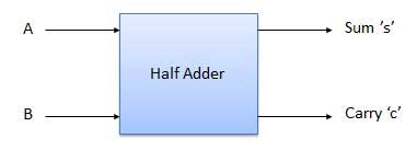 Truth Table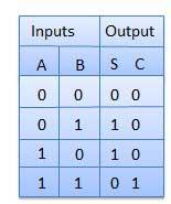 Circuit Diagram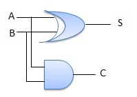
Full adder is developed to overcome the drawback of Half Adder circuit. It can add two one-bit numbers A and B, and carry c. The full adder is a three input and two output combinational circuit.
Block diagram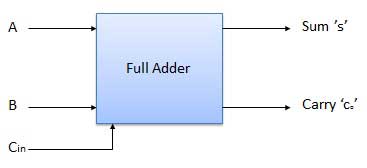 Truth Table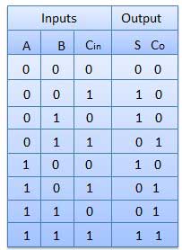 Circuit Diagram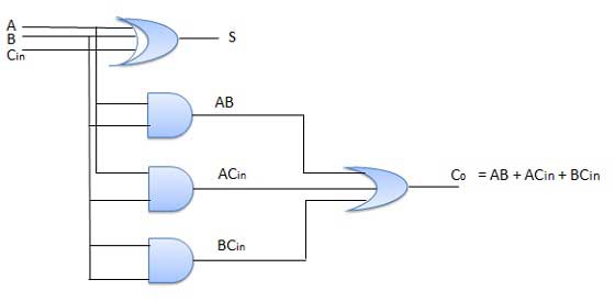
2. Multiplexer
Multiplexer is a special type of combinational circuit. There are n-data inputs, one output and m select inputs with 2m = n. It is a digital circuit which selects one of the n data inputs and routes it to the output. The selection of one of the n inputs is done by the selected inputs. Depending on the digital code applied at the selected inputs, one out of n data sources is selected and transmitted to the single output Y. E is called the strobe or enable input which is useful for the cascading. It is generally an active low terminal that means it will perform the required operation when it is low.
Block diagram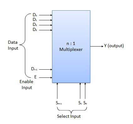
Multiplexers come in multiple variations
Block Diagram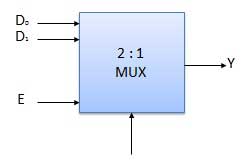 Truth Table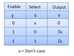
3. Decoder
A decoder is a combinational circuit. It has n input and to a maximum m = 2n outputs. Decoder is identical to a demultiplexer without any data input. It performs operations which are exactly opposite to those of an encoder.
Block diagram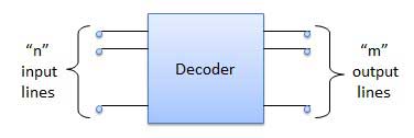
Examples of Decoders are following.
2 to 4 Line Decoder
The block diagram of 2 to 4 line decoder is shown in the fig. A and B are the two inputs where D through D are the four outputs. Truth table explains the operations of a decoder. It shows that each output is 1 for only a specific combination of inputs.
Block diagram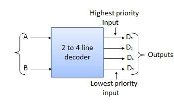 Truth Table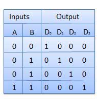 Logic Circuit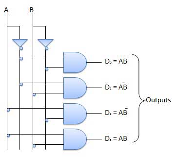
4. SR Flip Flop
It is basically S-R latch using NAND gates with an additional enable input. It is also called as level triggered SR-FF. For this, circuit in output will take place if and only if the enable input (E) is made active. In short this circuit will operate as an S-R latch if E = 1 but there is no change in the output if E = 0.
Block Diagram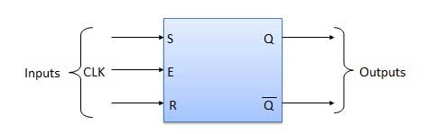 Circuit Diagram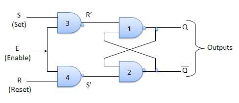 Truth Table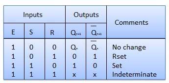 Operation
 |

0 Comments:
Post a Comment